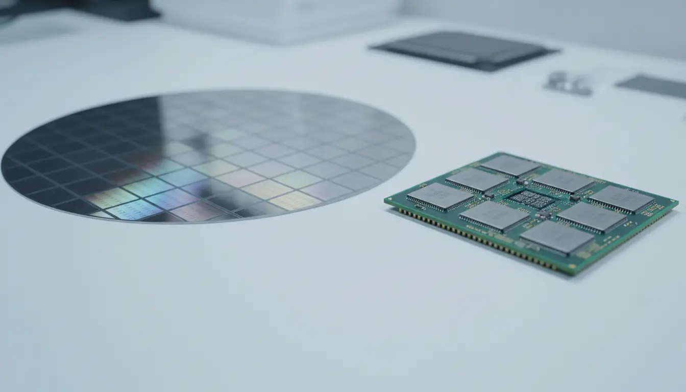

Chiplet Architecture: The Future of Modular CPU/GPU Design
The semiconductor industry is undergoing one of its biggest architectural shifts in decades, and at the center of this transformation is chiplet architecture. Instead of building a single, large, monolithic chip, manufacturers are increasingly turning to modular CPU and GPU design composed of multiple smaller dies—called chiplets—packaged together to function as a single processor. This approach is revolutionizing how high‑performance computing, gaming, AI workloads, and data centers are designed and scaled.
What Is Chiplet Architecture?
Chiplet architecture is a design methodology in which a processor is built from several smaller integrated circuits (dies), each responsible for specific functions. These chiplets are interconnected using high‑speed interfaces inside a single package. From a system’s perspective, the resulting processor behaves like a single coherent CPU or GPU, but internally it is a collection of modular building blocks.
In traditional monolithic CPU design, all cores, cache, memory controllers, and I/O logic are fabricated on a single piece of silicon. As chips grow in complexity, this model becomes harder to sustain due to manufacturing limits, yield issues, and escalating costs. Chiplets solve these challenges by breaking the design into more manageable units.
Why Chiplets Instead of Monolithic Chips?
There are several strategic and technical reasons driving the move toward chiplet‑based processors:
- Better Manufacturing Yield and Lower Cost
Large dies are more prone to defects during fabrication. A single defect can render the entire chip unusable. By contrast, smaller chiplets have statistically higher yields because the probability of a defect affecting each individual die is lower. Even if one chiplet is faulty, it can often be discarded without wasting the entire multi‑chip package. This translates into more usable chips per wafer and lower cost per functional processor. - Scalability and Flexibility
Modular CPU and GPU design makes it easier to scale performance. Need more cores? Add more compute chiplets. Need better I/O? Pair existing compute chiplets with new I/O dies without redesigning the entire architecture. This scalability is especially attractive for data centers and cloud providers that require fine‑grained performance tiers. - Mix‑and‑Match Process Nodes
One of the biggest advantages of chiplet‑based processors is the ability to manufacture different chiplets on different process nodes. High‑performance compute cores can be built using cutting‑edge process technologies, while analog components, I/O, and memory controllers can remain on more mature and cost‑effective nodes. This heterogeneous integration significantly improves cost‑performance balance. - Shorter Time to Market
Reusing validated chiplets across product lines reduces design risk and accelerates development cycles. A company can build a product portfolio from a library of reusable die components instead of starting from scratch for every generation.
How Chiplet‑Based CPUs and GPUs Work
From a high‑level viewpoint, chiplet‑based CPUs and chiplet‑based GPUs typically consist of:
- Compute Chiplets (Core Complexes):
These contain CPU cores or GPU compute units, along with portions of cache. - I/O or System Chiplet:
This die manages connectivity such as PCIe, memory controllers (DDR, HBM, etc.), USB, and other interfaces. - High‑Speed Interconnect:
A specialized on‑package interconnect (sometimes a proprietary protocol, sometimes based on emerging standards like UCIe) links the chiplets together. The goal is to provide bandwidth and latency characteristics as close as possible to an on‑die connection. - Package Substrate or Interposer:
The chiplets are mounted on an advanced package substrate, organic substrate, or silicon interposer that provides physical and electrical connectivity.
Careful chiplet interconnect design is crucial. If bandwidth is too low or latency too high, performance will suffer and the benefits of modularity will be lost. This is why advanced packaging technologies—such as 2.5D, 3D stacking, and through‑silicon vias (TSVs)—are becoming increasingly important.
Advantages of Modular CPU/GPU Design
Chiplet architecture introduces several significant technical benefits:
- Performance Per Watt Optimization
By choosing the optimal process node for each chiplet, designers can reduce power consumption while boosting performance. Compute cores may run on a dense, energy‑efficient node, while analog functions remain on nodes better suited to voltage and signal integrity. - Customized Solutions for Different Markets
With a modular CPU design, vendors can create a range of products by combining chiplets in various configurations. For example, a data‑center processor can feature many compute chiplets and large I/O capabilities, while a consumer‑grade CPU can use fewer chiplets to hit specific power and price targets. - Improved Reliability and Binning
Because multiple chiplets are tested individually, manufacturers can “bin” them based on performance characteristics. High‑performing chiplets go into premium products, while lower‑performing but still functional dies can power mainstream SKUs, increasing overall utilization. - Future‑Proof Upgrades
As standards like UCIe gain traction, it may become possible to integrate chiplets from different vendors in the same package. This could lead to plug‑and‑play ecosystems for specialized accelerators, AI engines, and security modules in future multiprocessor designs.
Challenges and Trade‑Offs
Despite its promise, modular chip design is not a silver bullet. It introduces its own set of complexities:
- Packaging Complexity and Cost
Advanced packaging is both technically challenging and more expensive than traditional packages. Fine‑pitch interconnects, alignment accuracy, and thermal considerations all add engineering overhead. - Signal Integrity and Latency
On‑package communication, while fast, is still not quite as seamless as on‑die wiring. Designers must carefully manage signaling, clocking, and power delivery to minimize latency penalties and maintain bandwidth. - Design and Validation Overhead
Multi‑die systems require sophisticated verification flows, especially for coherence, cache consistency, and inter‑chip communication. This increases non‑recurring engineering (NRE) costs. - Thermal Management
Distributing heat across multiple chiplets can help in some scenarios, but it also complicates heatsink and cooling design. Hotspots on specific chiplets may demand more advanced thermal solutions.
Chiplet Architecture in Data Centers and AI
For data‑center workloads and AI accelerators, chiplet architecture is particularly appealing. High‑performance computing systems often demand huge core counts, large memory bandwidth, and flexible I/O configurations. With a multi‑chip module (MCM) design, cloud providers can deploy CPUs and GPUs tuned for specific workloads, such as:
- AI training and inference
- Large‑scale databases and analytics
- High‑throughput networking and storage
By mixing compute chiplets, high‑bandwidth memory chiplets, and networking chiplets in one package, vendors can deliver tightly integrated solutions with better energy efficiency, lower latency, and more predictable performance.
The Future of Chiplet‑Based Processors
The industry is moving toward a more open ecosystem for chiplet‑based processors, driven by emerging interconnect standards and collaboration between foundries, IP vendors, and system integrators. As design methodologies mature, chiplet adoption is likely to expand beyond flagship CPUs and GPUs into embedded systems, automotive computing, and even edge devices.
In the long term, chiplets could enable a “Lego‑style” approach to silicon, where companies assemble customized processors from a catalog of interoperable dies. This will redefine how performance, cost, and power are balanced in modern computing platforms.