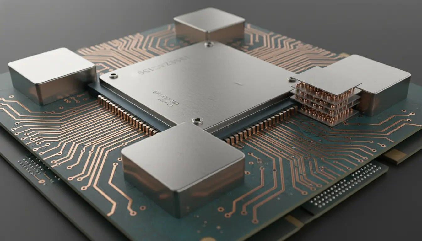

As data-intensive workloads surge across AI, high-performance computing (HPC), graphics, and networking, traditional memory architectures are hitting bottlenecks in bandwidth, latency, and energy efficiency. 3D stacked memory—often referred to as high-bandwidth memory (HBM)—addresses these constraints by vertically integrating multiple DRAM dies connected with through-silicon vias (TSVs) and mounted close to the processor via a silicon interposer. This architectural shift drastically increases memory bandwidth while reducing power per bit, enabling faster training of large AI models, smoother real-time analytics, and more responsive high-fidelity graphics.
This article explains how 3D stacked memory works, why high bandwidth matters, key design trade-offs, emerging standards, and where the technology is headed. It’s optimized for SEO, with natural use of related terms to help search engines understand the topic contextually.
What Is 3D Stacked Memory?
3D stacked memory is a packaging approach that vertically stacks multiple memory layers (dies) to create a compact, high-density memory subsystem. Instead of placing DRAM chips side-by-side on a PCB, manufacturers stack them and connect layers using TSVs—tiny vertical conduits that allow high-speed, low-latency communication between layers. When paired with a wide interface and positioned near the CPU or GPU on a silicon interposer, the result is high-bandwidth memory that can feed compute units at rates that far exceed traditional DDR or GDDR.

Key elements:
- Stacked DRAM dies: Multiple memory layers bonded and connected vertically.
- TSVs and micro-bumps: Provide dense, high-speed interconnects.
- 2.5D packaging with interposer: Places memory and compute dies side-by-side on a passive silicon interposer for short, wide connections.
- Wide I/O interface: Thousands of data lines operating at moderate per-pin speed to achieve very high aggregate bandwidth.
Why High Bandwidth Matters
Modern workloads are overwhelmingly memory-bound. Training transformer-based AI models, running graph analytics, simulating physics at scale, and rendering 4K/8K scenes all require moving enormous amounts of data quickly. The compute units (GPU/TPU/AI accelerator cores) often sit idle waiting on data. By dramatically widening the interface and shortening the communication path, 3D stacked memory:
- Increases effective throughput so compute cores stay busy.
- Reduces memory latency variance, improving predictability.
- Cuts energy per bit transferred, which reduces total cost of ownership at scale.
- Enables larger, more complex models and datasets to be processed in real time.
How 3D Stacked Memory Achieves High Bandwidth
Bandwidth is a function of bus width and signaling rate. Traditional memory scales bandwidth primarily by increasing frequency, which raises power and signal integrity challenges. 3D stacked memory takes the opposite approach:
- Very wide buses (thousands of I/O signals) provide massive parallelism.
- Moderate per-pin data rates reduce power and simplify timing.
- Proximity to compute reduces trace length and parasitic losses.
- Multiple memory stacks can be used in parallel for linear bandwidth scaling.
For example, an HBM stack can deliver hundreds of GB/s per stack. Systems with multiple stacks can exceed a terabyte per second of memory bandwidth, a key enabler for training large AI models and running complex HPC workloads.
Power, Thermal, and Area Considerations
While 3D stacking boosts performance, it introduces new design trade-offs:
- Thermal management: Stacked dies concentrate heat. Advanced thermal materials, heat spreaders, and package-level cooling are essential.
- Power delivery: Many I/O lines and layers require robust, low-impedance power networks.
- Yield and cost: Stacking increases the cumulative impact of defects. Known good die (KGD) strategies and advanced testing mitigate risk but raise complexity.
- Interposer area: 2.5D packaging requires a silicon interposer large enough to host compute and multiple memory stacks, affecting cost and design constraints.
Despite these challenges, the performance-per-watt benefits are compelling for data centers and high-end edge devices.
3D Stacked Memory vs. DDR and GDDR
- DDR: Great for general-purpose systems, but limited by narrower interfaces and motherboard routing distances. Scaling bandwidth typically means higher frequencies and more channels, increasing complexity.
- GDDR: Widens interfaces and increases frequencies for GPUs, but still relies on PCB routing and higher per-pin speeds, which elevate power and signal integrity concerns.
- 3D stacked memory (HBM): Prioritizes an ultra-wide, lower-frequency interface located close to compute, delivering superior bandwidth-per-watt and reduced latency at the system level.
Use Cases and Industry Adoption
- AI training and inference: Large language models, recommendation systems, and computer vision workloads benefit from high throughput and lower memory stalls.
- HPC and scientific computing: CFD, molecular dynamics, weather forecasting, and seismic imaging demand sustained bandwidth.
- Graphics and visualization: Real-time ray tracing, VR/AR rendering, and film-quality pipelines see smoother frame times and higher fidelity.
- Networking and storage acceleration: Packet processing, encryption, and compression offloads achieve consistent low-latency performance.
- Edge AI and autonomous systems: Energy-efficient bandwidth is crucial where power and space are constrained.
Standards and Ecosystem
The high-bandwidth memory ecosystem includes successive generations improving capacity, throughput, and efficiency. As generations advance, we see:
- More memory dies per stack and higher per-pin rates.
- Improved controllers, error correction, and power management.
- Tighter integration with GPUs, AI accelerators, and specialized SoCs.
- Emerging chiplet-based architectures that mix-and-match compute and memory tiles on advanced interposers or using direct die-to-die links.
The industry is also exploring CXL-attached memory expansion for capacity scaling, potentially complementing stacked memory by offering tiered bandwidth and latency profiles in a unified memory architecture.
Design Best Practices
For teams considering 3D stacked memory, key recommendations include:
- Model bandwidth needs early: Profile workloads to quantify sustained and peak bandwidth and latency sensitivity.
- Balance stacks and channels: Right-size the number of stacks and channels to avoid underutilization or starvation.
- Optimize memory access patterns: Align data layouts with wide interfaces, minimize random access, and coalesce requests.
- Plan thermal from day one: Include realistic power and thermal simulations, airflow design, and material selections.
- Validate power integrity: Ensure robust delivery networks and decoupling strategies across the stack and interposer.
The Road Ahead
3D stacked memory will continue to be a cornerstone of heterogeneous computing architectures. As AI models scale and real-time analytics permeate more industries, the premium on bandwidth-per-watt and predictable latency grows. Expect further advances in TSV technology, improved yields, denser stacks, and tighter coupling between compute and memory through chiplet ecosystems. Together, these trends will push the boundaries of what’s possible in AI training, HPC simulations, and next-generation graphics—while keeping power budgets in check.
Conclusion
3D stacked memory delivers high bandwidth, energy efficiency, and predictable performance—exactly what modern data-intensive workloads demand. By vertically integrating memory and placing it next to compute with ultra-wide interfaces, organizations can unlock higher throughput, better utilization of accelerator cores, and faster time-to-results. For teams building AI, HPC, or advanced graphics pipelines, adopting 3D stacked memory is a strategic path to sustained competitive advantage.