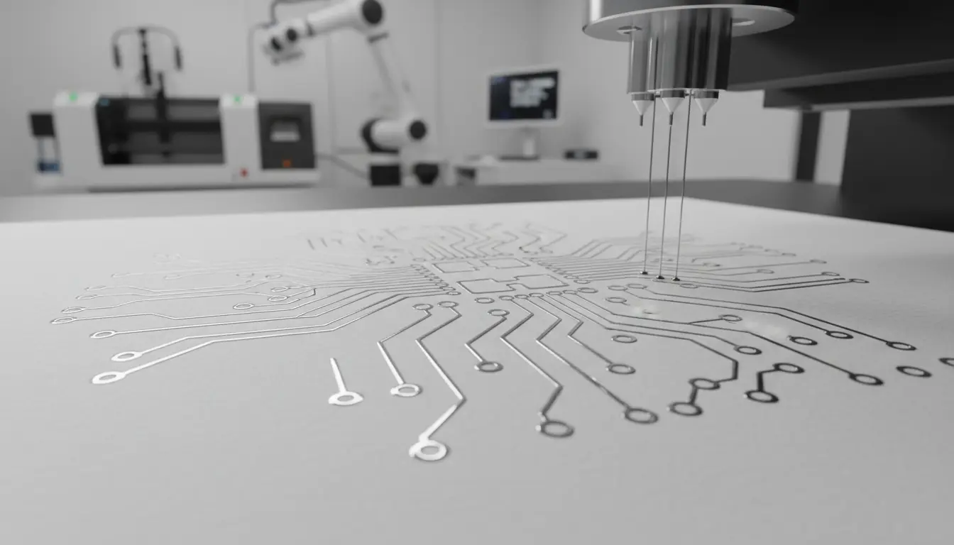

Paper-Based Inkjet Circuit Printing — Printing Electronics
Why Print Electronics on Paper?
Paper-based inkjet circuit printing turns a simple sheet into a working electronic platform. Instead of subtracting copper from fiberglass boards, you deposit conductive patterns exactly where you need them. This approach supports fast iteration, low material waste, and lightweight form factors that conventional PCBs struggle to match.
Teams use this method when they need quick prototypes, disposable sensors, interactive packaging, or classroom-friendly builds. You can also scale it for pilot manufacturing when your design tolerates the electrical limits of printed traces. When you treat paper as an engineering substrate—not stationery—you unlock a practical path into printed circuit technology without heavy tooling.
The Core Idea: Inkjet as a Circuit Fabrication Tool
Inkjet printing systems place tiny droplets with controlled volume and positioning. In electronics, those droplets contain conductive particles or conductive polymers. The printer follows a vector or bitmap pattern and performs circuit pattern deposition directly onto the surface. After printing, you cure the ink so it forms a continuous conductive path.
This workflow gives you a digital manufacturing loop: design → print → cure → test → revise. You keep cycle times short and costs predictable, especially for early-stage development where every change matters.
Conductive Inks: What Makes Them Work
Most successful projects start with the right conductive ink formulations. Inks must satisfy conflicting requirements:
- Flow smoothly through nozzles without clogging
- Wet the substrate evenly without bleeding
- Dry and cure into a stable conductive network
- Adhere to paper fibers and coatings
Many labs prefer silver nanoparticle inks because they offer high conductivity at relatively low printed thickness. You still need to cure them properly to get good particle-to-particle contact. Lower-cost alternatives exist, but they can demand higher curing temperatures or deliver lower conductivity—trade-offs you must accept up front.
If you target environmentally minded projects, you can also explore water-based formulations and approaches aligned with sustainable electronics production, but you should verify conductivity, shelf life, and long-term stability before committing to a design.
Choosing Paper: Not All Sheets Behave the Same
Paper substrate electronics depend heavily on surface chemistry and porosity. Standard copier paper absorbs liquids aggressively, which can blur edges and break fine traces. Coated papers often perform better because they limit absorption and keep lines crisp.
When evaluating paper, focus on:
- Surface smoothness (supports fine features)
- Absorption rate (controls spreading/feathering)
- Dimensional stability (humidity can warp paper)
- Coating compatibility (some coatings repel certain inks)
You can improve results with substrate preparation methods such as light surface cleaning, controlled humidity, or a thin primer layer designed for inkjet deposition. These steps sound small, but they often decide whether a trace becomes a reliable conductor or an inconsistent resistor.
A Practical Process Flow (Design to Working Circuit)
You can run a repeatable workflow even with modest equipment:
- Design for print realities
Printed traces rarely match copper’s performance. Increase trace width, shorten high-current paths, and avoid pushing power delivery through long printed lines. You’ll do electrical conductivity optimization through geometry as much as material choice. - Print test coupons first
Before you print a full circuit, print straight lines, pads, and serpentine resistors. Measure resistance and check adhesion. This quick step saves hours later. - Cure with control, not guesswork
Curing might involve heat, photonic curing, or chemical sintering depending on ink. Monitor time and temperature. Paper can scorch or warp, so you must balance conductivity gains with substrate safety. - Protect and encapsulate
Paper hates moisture. If the circuit must survive handling or humidity, add a protective layer (lamination film, conformal coating, or a thin polymer barrier) while preserving contact points. - Assemble with gentle methods
Traditional soldering can destroy paper or delaminate traces. Use conductive adhesives, low-temperature alloys (with caution), crimped contacts, or mechanical clamps.
This routine supports flexible electronics manufacturing in settings where speed and adaptability matter more than maximum electrical performance.
Where Paper-Based Printed Electronics Shine
Paper circuits win when the application values low cost, light weight, disposability, or surface area. Common, real-world uses include:
- Smart packaging sensors that detect humidity, tampering, or temperature exposure across supply chains
- RFID printed tags and antennas for inventory, event access, or simple tracking
- Wearable circuit devices for short-term demos, education, or low-power sensing patches
- Educational kits that teach circuits without etching chemicals or rigid boards
- Low-cost diagnostics where single-use biocompatible electronics reduce contamination risk
In many of these cases, you don’t need copper-like performance. You need “good enough” conductivity, consistent printing, and predictable behavior at low power.
Design Tips That Raise Reliability Fast
You improve success rates more with design discipline than with exotic materials.
- Use wider traces than you think you need. Paper movement, ink spread, and minor misalignment can create weak points.
- Favor rounded corners and gradual transitions. Sharp angles concentrate current and can crack under bending.
- Build pads large and tolerant. Assembly on paper demands bigger contact areas.
- Plan for bending. If the device flexes, route traces along neutral bend lines and avoid placing critical joints at fold points.
- Add redundancy where possible. Parallel traces or larger ground areas can prevent single-point failures.
These choices matter even more in multi-layer printing techniques, where via formation and interlayer adhesion introduce additional failure modes. If you move to multilayer, validate each layer’s resistance and alignment before stacking complexity.
Limitations You Must Acknowledge (And How to Work Around Them)
Paper-based circuits come with constraints. If you plan for them early, you can still ship successful products.
- Lower conductivity than copper: Printed lines often show higher resistance. Work around it with shorter runs, thicker prints, or wider traces.
- Environmental sensitivity: Humidity can change resistance and degrade adhesion. Add encapsulation and control storage conditions.
- Assembly challenges: Standard reflow soldering doesn’t fit paper well. Switch to conductive epoxies or press-fit approaches.
- Durability and abrasion: Exposed traces scratch easily. Protect them if users will handle the device.
When you treat these as design inputs—not surprises—you can pick realistic use cases and avoid overpromising performance.
What the Future Looks Like
As materials improve, paper-based inkjet printing expands beyond novelty. Better inks, smarter curing methods, and improved coatings will raise consistency and reduce cost. We will also see tighter integration with low-power electronics, printed antennas, and disposable sensing platforms. The biggest wins will come from system-level design: circuits, packaging, and data collection designed together, not bolted on later.
When engineers align printed circuit technology with the strengths of paper—lightweight, cheap, flexible, and scalable—the results become commercially meaningful, not just experimental.
Amazon.com Product Recommendation (1 item)
Product suggestion: Search on Amazon.com for “Bare Conductive Electric Paint (conductive ink)”. It’s commonly used for beginner-friendly conductive printing and quick experiments on paper.